In the consumer segment, main memory or DRAM is broadly categorized as DDR and LPDDR, short for Dual Data Rate and Low Power Dual Data Rate, respectively. The former is used in desktops and high-end laptops, while smartphones and ultrabooks leverage the latter. AMD Ryzen 7000 mobile and Intel Core Ultra CPUs support both standards, depending on the form factor. The 28-45W models use DDR5, while their 9-15W counterparts use LPDDR5 memory for improved power efficiency.
- DDR4 was the defacto memory for PCs over the last decade, with data rates of up to 3,200 Mbps. Its successor, DDR5, started with a base transfer rate of 4,800 Mbps but has increased to 6,400 Mbps. Overclocked variants go as high as 7,200 Mbps.
- LPDDR4 (and LPDDR4X) supported data rates of up to 4267 Mbps and has largely been replaced by LPDDR5 and LPDDR5X. LPDDR5 typically offers a data rate of up to 6400 Mbps, while LPDDR5X should up it to 8,533 Mbps.
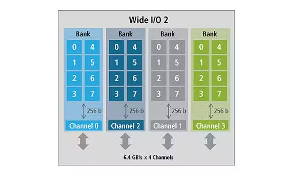
LPDDR5 is one of the most power-efficient memory standards. Thanks to Dynamic Voltage Scaling (DVS), LPDDR5 supports two voltage modes: 1.05V (C) and 0.5V (I/O) while operating at higher frequencies and 0.9V (C) and 0.3V (I/O) when idle. Like LPDDR4/4X, LPDDR5 features 2x 16-bit channels and a burst length of 16 per channel. Burst lengths of 32 are also supported in some configurations.
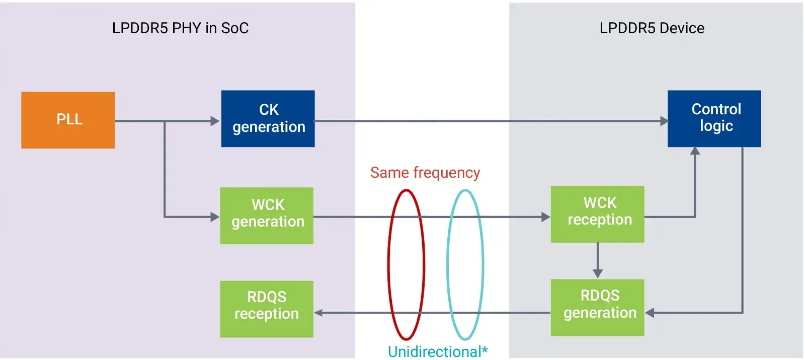
LPDDR4 and LP4X support two Frequency Set Points (FSPs) for C/A (Command/Address) and DQ while LPDDR5 bumps it up to 3, allowing for rapid switching across the three frequencies at extremely low power. Another power-saving technology, Write X allows the transfer of certain bit patterns to contiguous memory locations without toggling the DQ bits on the channel.
Burst-length: When the CPU or cache requests new data, the address is sent to the memory module and the needed row, then the column is located (if not present, a new row is loaded). Keep in mind that there’s a delay after every step.
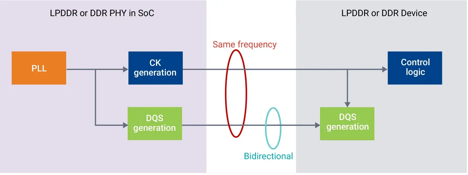
After that, the entire column is sent across the memory bus in bursts. For DDR4, each burst was 8 (or 16B). With DDR5, it has been upgrades to 16 (up to 32B). There are two bursts per clock and they happen at the effective data rate. Furthermore, similar to LPDDR4, DDR5 has 2x 32-bit channels per DIMM for a total of four channels in a dual-DIMM configuration. The prefetch and BL have also been increased to 16. This figure is ideal as each cache line in memory is of the same size.
| LPDDR5 | DDR5 | |
|---|---|---|
| Memory Size (per channel) | 2Gb to 32Gb | 8Gb to 64Gb |
| Burst Length | 16 | 16 |
| Prefetch | 16n | 16n |
| Banks | 16 | 32 |
| Speed | Up to 6400 Mbps | Up to 8400 Mbps |
| Voltage | 1.05V/0.9V core 0.5V/0.3 V I/O | 1.1V VDD 1.8V VPP |
DDR5 features 2x 32-bit channels per DIMM (DDR4 had one 64-bit per channel), with a burst length of 16 and a prefetch of 16n per channel (DDR4 had half as much). DDR5 and LPDDR5 support speeds of up to 6400 Mbps per the JEDEC standard. We’re already seeing overclocked DDR5 modules hit 7,200 Mbps and higher, something LPDDR5X should also achieve.
LPDDR5 supports memory densities of up to 32Gb per channel, while DDR5 can go as high as 64Gb. Both support the same 16n prefetch and a 16-beat burst length per transaction.
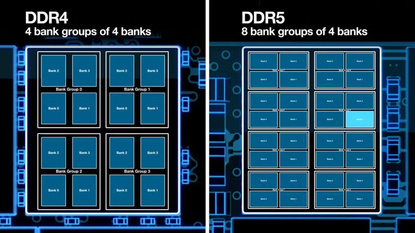
DDR5 has a complex memory bank structure with 32 banks per channel. These are divided into eight bank groups of four banks each. LPDDR5 has a more flexible bank architecture. It supports three bank modes: four banks with four bank groups (bank group mode), eight banks, and sixteen banks.
The bank group mode allows transfer rates higher than 3,200Mbps alongside burst lengths of 16 or 32. The eight-bank mode allows all transfer rates with a burst length of 32, while the sixteen-bank mode is for bandwidths under 3,200Mbps with a burst length of 16 or 32.